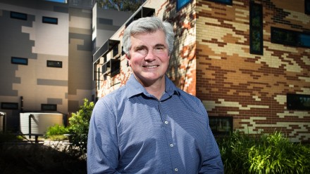
Associate Professor Fiona Beck

Contacts
A/Prof Beck’s research focuses on the opportunities and challenges in transitioning the global energy system from fossil fuels to renewable energy.
A/Prof Beck is the Research Lead for the Facilitating Transformation Program in the HILT Cooperative Research Centre - De-Risking Decarbonisation for Heavy Industry. HILT CRC delivers rigorous, targeted, and industry-led research aimed at resolving the challenges facing the iron/steel, alumina and cement/lime sectors during the net-zero transtion. She previously led the ANU's Hydrogen Fuels project as part of the Zero Carbon Energy for the Asia-Pacific Initiative (ZCEAP). Her work combines engineering, energy policy, and techno-economics to provide high quality information on the costs, benefits, and implications of decarbonisation pathways for a range of industry and government stakeholders. As such, she has contributed significantly to the national conversation on new, zero-carbon industries and exports, through academic publications, presentations to stakeholders, submissions to government, and contributions in the media.
A/Prof Beck has a background in applied physics (MSci 2006, University of Glasgow) and engineering (PhD 2011, ANU), and has previously held prestigious international fellowships including a Marie Curie Fellowship from the European Commission (IIF, 2012), and a Discovery Early Career Researcher Award (DECRA, 2018) from the Australian Research Council. She has over 15 years’ experience developing technologies for renewable energy including solar cells and the production of renewable fuels and commodities like hydrogen and ethylene. Her research in this area leverages a deeper understanding of light-matter interactions on the nanoscale to design novel photovoltaic and photo(electro)chemical devices. Currently, her group is working on systems for carbon dioxide reduction.
Research interests
- Energy system modelling for the low carbon transition
- Energy policy and technoeconomic analysis for decarbonisation of renewable fuels, chemicals and heavy industry
- Photosynthesis and photoelectrochemistry for renewable fuels
- Hot electron science and nanophotonics
Groups
- Researcher, Solar photovoltaics
- Researcher, Renewable fuels
- Researcher, Hydrogen economy
- Researcher, Industrial decarbonisation
Projects
- Convenor, Hydrogen Fuels program
- ANU Research Team contributor, Regulatory Frameworks for Renewables-based Trade and Investment program
- ANU Research Team contributor, Renewable Energy Systems program


